


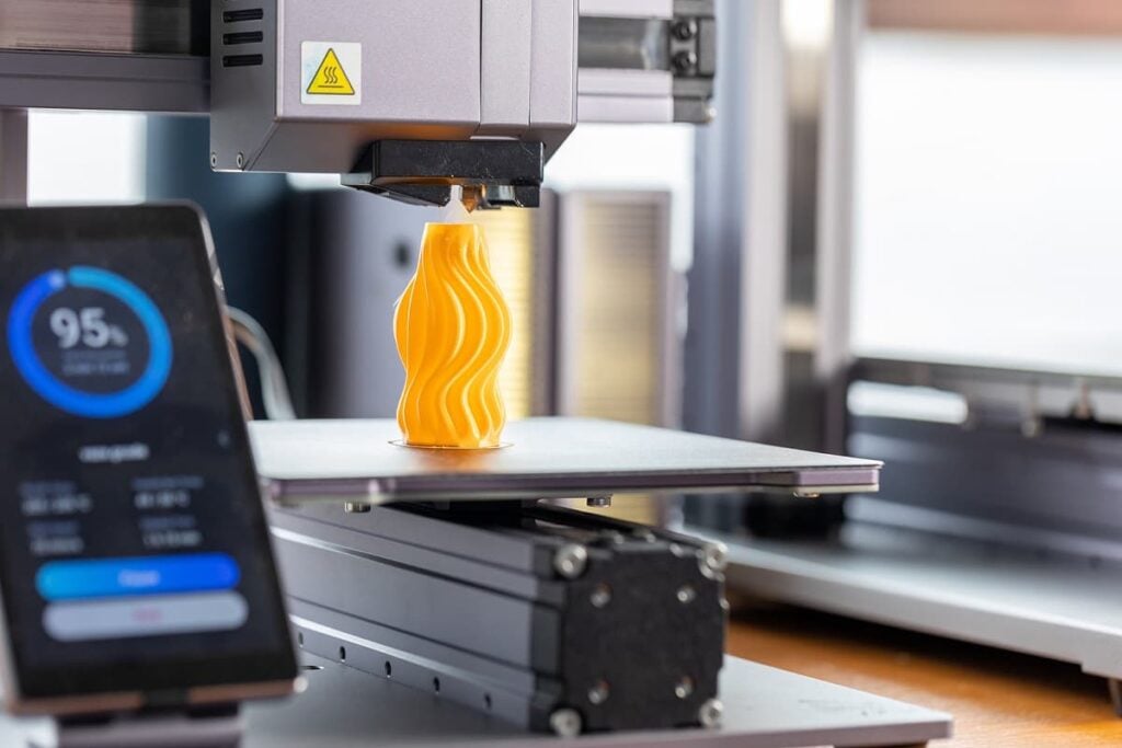
A Nano 3D Printer That Prints Nano-Sized Objects


Table of contents
In a recent article, we wrote about an Israeli 3D printing startup that’s developing their flagship machine “capable of micron-resolution printing, with the capability to print thousands of parts in a single build.” The ability to 3D print objects at a micro or nanoscale opens doors for many new applications. Today, we’re going to look at Nanoscribe, a company that’s built the “world’s highest resolution 3D printer designed for ultra-precise and rapid microfabrication.”
About Nanoscribe
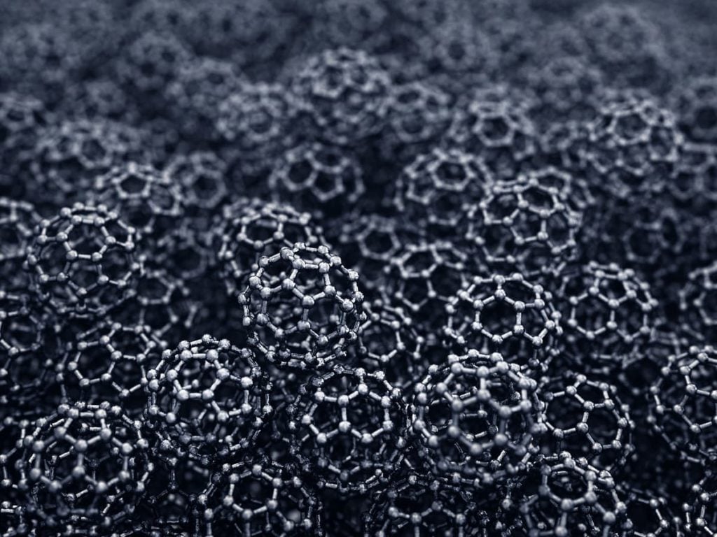
Spun off from the Karlsruhe Institute of Technology in 2007, Nanoscribe’s founders are leading scientists in the field of nanophotonics. In other words, they’re experts in studying how light behaves at a nanoscale. (That’s one of the things that makes nanotechnology so interesting. Under 100 nanometers, everything starts to behave differently.) The German company has raised an undisclosed amount of funding to build what they’re calling the “highest resolution commercially available 3D printer” dubbed the “Photonic Professional GT2” which can create structures just 30 nanometers across. (To put this in scale, a human blood cell is 8000 nanometers across.) In August of last year, they opened an office in ‘Murica (Bahstun to be exact) and three months later sold their 200th machine. Let’s try to understand what their nano 3D printers do and the technology that powers them.
Two-Photon Polymerization
They say that you should be able to explain your business plan to a nine-year-old – during the duration of a 30-second elevator ride. For Nanoscribe, they create very tiny 3D objects that can’t even be seen with the naked eye using photons, the basics units of light. The technique is called 2–Photon Polymerization (2PP) and it’s kind of cool to visualize. Some fellow who wrote a book on the topic describes the process as follows:
The technique is also referred to as two-photon polymerization because the polymerization of the photoresist is initiated by a two-photon process—that is, it requires the absorption of two photons at the same location simultaneously (or within a very short time of one another). This only occurs in a small volume at the center of the laser focus where the intensity is high enough. By sweeping the laser beam through the photoresist, optical quality 3D structures can be reproducibly fabricated with voxel sizes down to ∼ 100 ×100 × 300 nm3.
Credit: Light Robotics: Structure-Mediated Nanobiophotonics
Nanoscribe offers an entire product family of resins and other materials that can be used to print the tiniest structures on a variety of different substrates like glass, silicon wafers, photonic, and microfluidic chips. The Nanoscribe website contains stories of some very remarkable applications for the technology including:
- A filtering membrane that can capture circulating tumor cells
- A 3D printed scaffold that enables tailor-made neuronal networks
- A 3D-printed microscaffold cochlear implant
- Self-propelled microscopic donuts that can transport particles
- The world’s smallest microstents made of soft and responsive components
- A 3D printed micro valve for treating glaucoma (see below)

In addition to the above examples, here are some areas of research that 2PP technology is actively being used in.
- Microfluidics – Various microfluidic elements such as filters, mixers, and capillary pumps
- MEMS Devices– Remotely controlled movable micromachines can be printed with the device
- Biomedical Engineering – Their users commonly fabricate 3D scaffolds to study cell growth, migration or stem cell differentiation on biomimetic structures
- 3D Microoptics – Single micro-lenses, freeform optics, and compound lens systems can be printed without the need of post-print assembly

In addition to the Photonic Professional GT2 printer, Nanoscribe is also developing another machine that does equally cool things.
Nanoscribe’s Quantum X
The Nanoscribe Quantum X is the self-described “world’s first Two-Photon Grayscale Lithography system for maskless microfabrication of refractive and diffractive microoptics.” There’s a lot going on here, so let’s break down each item. We already understand how 2PP technology works for 3D printing, so how does it work for lithography? In fact, what is lithography anyways?
The entire semiconductor industry revolves around creating low-cost silicon chips that contain hundreds of millions of transistors using a technique called lithography. It’s best described as follows:
Lithography is the main tool used in IC manufacturing to record a binary image (pattern) on a layer of photosensitive material (photoresist) spun over a substrate, generally a semiconductor wafer.
Credit: Reference Module in Materials Science and Materials Engineering, 2016
There’s also something called “maskless lithography” which means you can skip some steps in the process which makes it easier to do research for low-volume, special purpose manufacturing. (This is literally the primary value proposition behind 3D printing – create prototypes quickly without having to create an entire manufacturing line to do so.) Turns out that something called “Beer’s law” imposes strong limitations on today’s maskless lithography devices. Nanoscribe has been able to bypass these limitations with their new machine which was released in Summer of 2019 and appears to be taking reservations still.

The fully-automated system uses a software wizard to guide designers and engineers through print job creation along with three cameras to monitor the progress.
Nanoscribe’s Growth
Nanoscribe isn’t a funded startup because they appear to be cash-flow positive having achieved profitability for twelve years in a row now while plowing back 25% of revenues into R&D. The company’s 70 employees provide the hardware, software, materials, and processes as a complete solution to more than 1,500 active operators of their systems located in over 30 countries. A key partner and investor for Nanoscribe is Carl Zeiss AG, a German manufacturer of optoelectronics and optical systems with over 7 billion in revenues for 2018. Says Nanoscribe, “ZEISS has supported Nanoscribe from the very beginning with technology and consulting and also made a major financial contribution through the acquisition of shares in September 2008.”
Conclusion
At some point, the investment community lost the term “nanotechnology” and just started to call it by different names. In a past article titled “Ginkgo Bioworks – Nanobots Are Finally Here,” we talked about how various aspects of synthetic biology bear a strong resemblance to how nanotechnology was originally envisioned by Eric Drexler in his book Engines of Creation. Ginkgo believes that biology itself is the most efficient manufacturing method on this planet, and they’re using it to create new organisms that do mankind’s bidding.
In the case of Nanoscribe, they’re able to create smooth 3D structures at a nano-level which is an incredible accomplishment. Much of this work appears to be in early stages, and the company mentions their research being highlighted in more than 700 peer-reviewed journal publications. Remember all that talk about nanobots? If you were going to build one, you’d probably want to start by looking at what Nanoscribe’s nano 3D printers can do.
Share


Interested in high resolution nanoprinting for solar cell applications.
Who is using your tool for this application at the nanoscale?
Hello Professor. You’ll need to reach out to the company directly as we’re just a research firm. Thank you!